Tailored surfaces
Nanometer-precision shaping of complex surfaces for optics and microelectronics
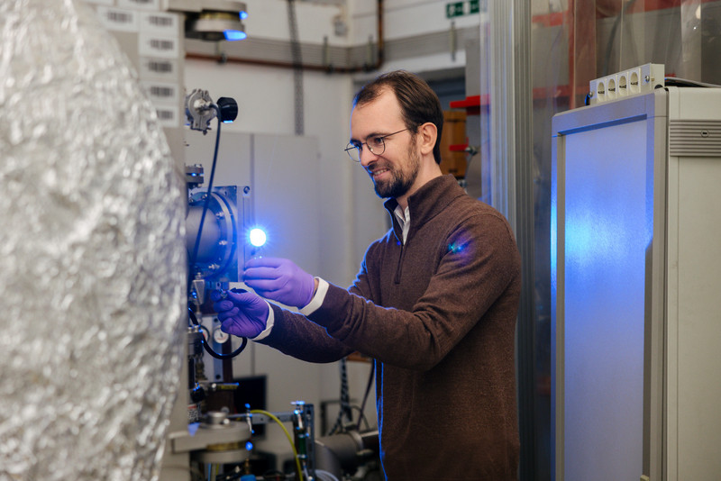
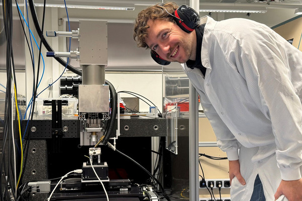
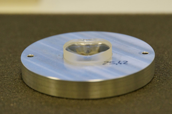
Applications in precision optics and microelectronics require surfaces with accuracies down to the nanometer and sub-nanometer range. At the IOM, beam-based methods are being developed for this purpose that enable targeted, non-contact shaping of complex surfaces.
Technologies and methods for precision shaping
- Development of ultraprecise machining processes based on
ion beams (ion beam figuring) and reactive plasma etching - Combination of plasma and laser processes for hybrid manufacturing technologies
- Investigation and modeling of the interactions between the beam and the material at the atomic level
- Optimization of beam tools for different materials and applications
Applications in optics, microelectronics, and photonics
- Fabrication and correction of aspheric and free-form optics
- Optical components for semiconductor manufacturing, high-power lasers, and photonics
- Precision surfaces for demanding applications in industry and research
From process modeling to application
- Deterministic machining based on simulations and process models
- Precise control of shape, structure, and roughness across all relevant scales
- Applicable to optical glass, ceramics, and metals
- Combining fundamental understanding with technological implementation
Projects
Al-ION - Optimization of diamond-machined RSA-Al501 surfaces for optical applications through process-integrated ion beam processing
This project investigates the fabrication of highly efficient metal optics for applications in the UV-VIS range using a process chain consisting of ultraprecision machining followed by ion beam processing. The goal is to better understand the cause-and-effect relationships between the two process steps, particularly with regard to the changes in the edge zone properties of fine-grained RSA-Al501 alloys resulting from diamond-supported machining. In collaboration with TU Berlin, the effects of these changes on ion beam-based smoothing and ablation processes are being analyzed. Based on this, process strategies and parameters for shape correction and surface optimization will be developed. The goal is to achieve roughness values below Rq < 0.5 nm with shape deviations below 2 nm.
Funded by the DFG
ECRION - Development and characterization of a compact, reactive-gas-compatible ECR ion beam source
This research project aims to develop a novel, reactive-gas-compatible, microwave-excited ion beam source for the ultraprecise processing of optical surfaces and semiconductor materials. It addresses key challenges such as long-term stability, energy efficiency, gas usage, and the precise control of beam current density and beam shape. The goal is to increase process performance by a factor of more than 10. The project encompasses the design, construction, and implementation of the ion source, as well as its electrical, microwave, and beam physics characterization. In addition, microwave coupling, plasma generation, ion extraction, and beam shaping are being investigated using simulation-based methods. The goal is to develop a functional ECR ion beam source prototype with a beam width of approximately 5 mm and a beam current of 20 mA, as well as an associated digital twin.
Funded by EFRE/SAB

TRADES - Training & Research in Advanced Dispersion-Engineered Grating-Waveguide Structures
The doctoral training network, comprising eight European partners, addresses the current shortage of skilled professionals in the field of photonics through a structured research and training program for doctoral students. As part of the program, 15 doctoral students are developing innovative optical components based on waveguide structures with subwavelength gratings for high-power laser applications. State-of-the-art deposition, lithography, and etching techniques are used to optimize manufacturability, efficiency (> 99.9%), and laser damage threshold (> 1 J/cm²) for sub-picosecond pulses. At the IOM in particular, ion beam methods for fabricating diffractive structures are being investigated. In addition, the fellows receive practical training in innovation management, entrepreneurship, and commercialization to prepare them for careers in photonics research and development.
Funded by the EU and Mediation Centre Stakeholder Network (MCSN)

RIBF 1000 - Ion Beam Processing Platform
Through the “Europe Supports Saxony” call for proposals, the Free State of Saxony (Sächsische Aufbaubank – SAB) is investing approximately 2 million euros from the European Regional Development Fund (ERDF) in the expansion of the research infrastructure at the IOM. This will strengthen the IOM’s innovative capacity and increase its national and international visibility. The goal of the project is to establish an ion beam processing platform at the IOM that, for the first time, will enable the investigation of chemically reactive processing methods (Reactive Ion Beam Figuring, R-IBF) on optical substrates with dimensions of up to 1 m² and to develop innovative deterministic (i.e., CNC-residence-time-controlled) methods for ultraprecise shape correction, ultra-smoothing, and micro-/nanostructuring of surfaces. The focus is particularly on machining processes for the production of astronomical and laser optics. The aim is to significantly expand the potential of ion beam machining technology in the fields of optics, photonics, and semiconductor manufacturing beyond the current state of the art.
Funded by EFRE/SAB
tigeR - Multiscale Crack Characterization in Optical Manufacturing
In collaboration with scientists from EAH Jena, this research project investigates methods for characterizing near-surface damage in optical surfaces, known as subsurface damage (SSD). The goal of the research project is to address the problem of defect characterization in the optics and glass industries by developing a non-destructive measurement method (optical coherence tomography, OCT). As part of the project, the OCT measurement method will be validated and optimized through depth-resolved preparation of crack damage using reactive plasma jet and ion beam etching. Finally, process chains for the fabrication of low-defect optics using ultra-fine grinding and plasma jet-assisted polishing will be evaluated.
Gefördert durch IGF / F.O.M.
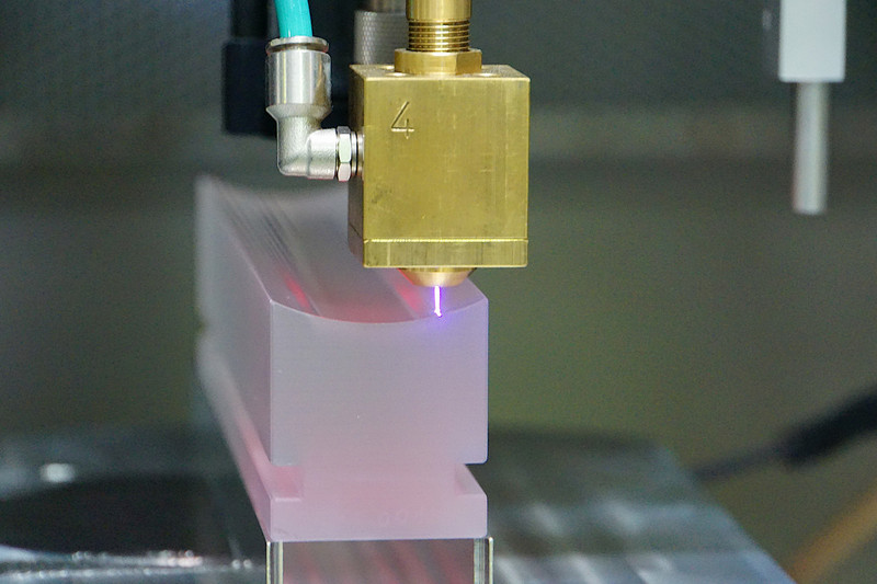
LasPlasJet - Laser-stimulated reactive atmospheric-pressure plasma jet etching processes for ultra-precision machining of optical glasses
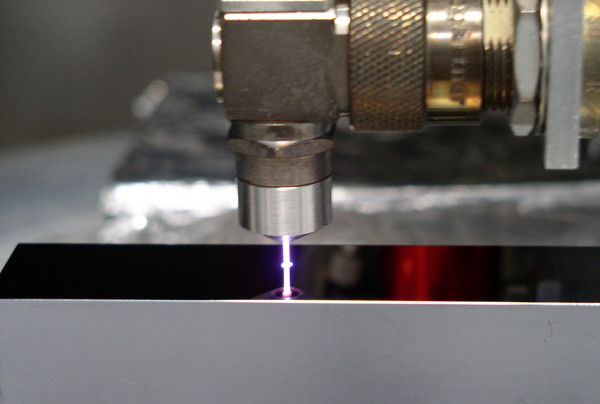
The LasPlasJet project investigates fundamental mechanisms involved in laser-assisted reactive atmospheric-pressure plasma jet etching of optical glasses and glass-ceramics. The materials considered in the project, such as N-BK7 and Zerodur, contain metal oxides that form non-volatile reaction products during plasma jet etching, making it impossible to achieve uniform, time-constant material removal that preserves surface roughness. By applying additional energy via laser radiation before, during, or after plasma etching, the aim is to specifically influence the ablation process and thereby improve the etch rate, etch selectivity, surface roughness, and homogeneity to achieve precise machining.
Funded by DFG
Al-ION - Optimization of diamond-machined RSA-Al501 surfaces for optical applications through process-integrated ion beam processing
This project investigates the fabrication of highly efficient metal optics for applications in the UV-VIS range using a process chain consisting of ultraprecision machining followed by ion beam processing. The goal is to better understand the cause-and-effect relationships between the two process steps, particularly with regard to the changes in the edge zone properties of fine-grained RSA-Al501 alloys resulting from diamond-supported machining. In collaboration with TU Berlin, the effects of these changes on ion beam-based smoothing and ablation processes are being analyzed. Based on this, process strategies and parameters for shape correction and surface optimization will be developed. The goal is to achieve roughness values below Rq < 0.5 nm with shape deviations below 2 nm.
Funded by the DFG
Publication highlights
F. Hölzel, J. Bauer, T. Arnold
Roughness evolution of fused silica, Zerodur® and N-BK7® in reactive ion beam figuring processes
Surf. Interfaces 69 (2025) 106769, 10.1016/j.surfin.2025.106769
Reactive Ion Beam Figuring (RIBF) is an advancement of conventional Ion Beam Figuring (IBF) and enables the ultra-precise fabrication of optical components. This study investigates the influence of reactive processes on three common optical materials: quartz glass, N-BK7Ⓡ, and ZerodurⓇ. The results reveal material-specific processing limits for RIBF and simultaneously demonstrate significant time savings during processing compared to conventional IBF.
H. Müller, S. Henkel, Chr. Schulze, S. Frank, J. Bliedtner, Th. Arnold
Freeform surfaces manufactured with a combination of ultra-fine grinding and plasma jet polishing
J. Eur. Opt. Soc. Rapid Publ. 21 (2025) 12, 10.1051/jeos/2025007
To meet the growing demands of free-form manufacturing, the feasibility of a new process chain was investigated, in which multiple free-form grinding steps are combined with thermally induced plasma jet polishing. The results showed that the surface quality after ultra-fine grinding—in terms of shape accuracy, defects in the mid-frequency range, and roughness—was sufficient for the subsequent plasma jet polishing. The surface shape is preserved during plasma polishing, and a surface roughness of Sq < 0.5 nm can be achieved.
R. Heinke, L. Silhan, M. Ehrhardt, P. Lorenz, J. Zajadacz, J. Bauer, T. Arnold, M. Sery, K. Zimmer
Stability of masking materials for pattern transfer of lithographic masks into fused silica by atmospheric pressure plasma jet etching
Micro and Nano Eng. 28 (2025) 100309, 10.1016/j.mne.2025.100309
The transfer of structures from lithographic resist masks onto optical glass using reactive plasma jets at atmospheric pressure was investigated as a new approach to the microstructuring of optical surfaces. The etching rates of various photoresists and quartz glass were investigated as a function of the gas composition of the plasma jet. Finally, the transfer of a diffraction grating with a period of 15 μm, a depth of 230 nm, and a roughness of less than 2 nm RMS onto quartz glass using a plasma jet was demonstrated.
M. Ehrhardt, P. Lorenz, J. Zajadacz, R. Heinke, T. Arnold, K. Zimmer
Transfer of micron pattern with reactive atmospheric plasma jets into fused silica
Appl. Surf. Sci. Adv. 23 (2024) 100636, 10.1016/j.apsadv.2024.100636
The creation of microstructures on optical surfaces using atmospheric-pressure processes is of technological interest in various fields of application. Reactive etching with an atmospheric plasma jet was investigated as a method for transferring metal mask patterns into quartz glass. Line patterns with widths ranging from 2.5 µm to 50 µm were exposed to a scanning CF₄/O₂ plasma jet, which transferred the patterns—with a feature height of up to 3.5 µm—into the substrate material.
F. Hölzel, D. Rolón, J. Bauer, J. Kober, S. Kühne, F. Pietag, D. Oberschmidt, T. Arnold,
Reactive ion beam smoothing of rapidly solidified aluminum (RSA) 501 surfaces for potential visible and ultraviolet light applications
Surf. Interfaces 38 (2023) 102784, 10.1016/j.surfin.2023.102784.
Applications in the visible (VIS) and ultraviolet (UV) spectral ranges require optical elements made of aluminum alloys with surface roughness in the subnanometer range. The use of reactive ion beam etching with the process gases CF₄ and N₂ was investigated. It was shown that the difference in etching rates between precipitates and the base material—which depends on the ion incidence angle—has a positive effect on reducing the height of precipitates protruding from the surface. In terms of micro-roughness, a surface roughness of Sq = 0.9 nm was achieved.
Equipment
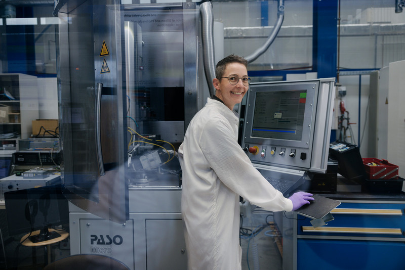
- PJM System: 5-axis plasma jet system for substrates up to 300 mm in diameter, reactive high-rate plasma jet etching source
- Profispeed PJM System Profispeed: 3-axis plasma jet system for substrates up to 300 mm in diameter, reactive fine-jet plasma jet source
- PJM System: 3-axis plasma jet system for substrates up to 400 mm, RF plasma jet source
- PJP System: 5-axis plasma jet system for plasma jet polishing processes, inert gas plasma jet source
- NTG200: Reactive-gas-compatible plasma jet and ion beam system for substrates up to 100 mm in diameter, fine-beam plasma source, various ion beam sources
- RIBF100: Reactive-gas-compatible ion beam processing system for substrates up to 100 mm in diameter, ECR fine-beam ion source
- NanoTech: IBF system for substrates up to 200 mm in diameter, RF ion beam source
- ASI Stitching Interferometer
- LuphoScan Optical Profiler
- CyberScan Optical Profiler
- PGI-Freeform Mechanical Profiler
Contact:

Prof. Dr. Thomas Arnold
Leiter Ultra-Präzisionsoberflächen
(Bevollmächtigter bei Abwesenheit des Vorstandes)