Tailored Surfaces
Nanometer-precision shaping and structuring for optics, photonics, and microelectronics
In the Ultra-precision Surfaces research area, the IOM develops beam-based technologies for processing precision surfaces with accuracies down to the sub-nanometer range, particularly for optical applications. This creates the essential prerequisites for key technologies - ranging from semiconductor lithography and high-power lasers to space optics.
Together, the research groups cover the entire process chain of ultraprecision surface processing - from the development and combination of beam-based methods, through targeted material processing, to application-oriented implementation in optical and photonic systems.

Prof. Dr. Thomas Arnold
Leiter Ultra-Präzisionsoberflächen
(Bevollmächtigter bei Abwesenheit des Vorstandes)


Technologies for ultra-precise surface processing
Beam-based processes and hybrid approaches
- Beam-based processes utilizing ion beams, plasma jets, and laser processes
- Non-contact processing through targeted material removal, smoothing, and texturing
- Combination and further development of hybrid processes (e.g., Plasma + Laser)
- Precise control of surfaces across all relevant lateral and vertical scales
Expertise across the entire process chain
From basic research to application
- Integration of experimentation, simulation, and modeling
- Development of technologies from tool design to application
- In-house research infrastructure with specialized radiation sources, machining equipment, and surface analysis
- Close collaboration with industry partners to facilitate practical implementation
Contributions to key technologies in digital and optical systems
Precision, scaling, and transfer
- Precision down to the sub-nanometer range
- Processing of structures ranging from a few nanometers to large areas
- A combination of basic research and technological implementation
- Contributions to digitalization, sensor technology, energy, and environmental technologies
Applications in key technologies
Applications in optics, photonics, and industry
- Optics for semiconductor manufacturing (EUV lithography)
- Components for photonics and high-power lasers
- Precision optics for space telescopes and sensor technology
- Functional surfaces for industrial applications
Technologies for ultra-precise surface processing
Beam-based processes and hybrid approaches
- Beam-based processes utilizing ion beams, plasma jets, and laser processes
- Non-contact processing through targeted material removal, smoothing, and texturing
- Combination and further development of hybrid processes (e.g., Plasma + Laser)
- Precise control of surfaces across all relevant lateral and vertical scales
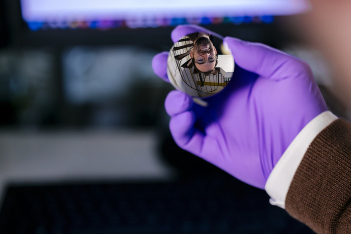
Ion Beam- and Plasma Jet-assisted Ultra-precision Shaping
Nanometer-precision shaping of complex surfaces for optics and microelectronics.
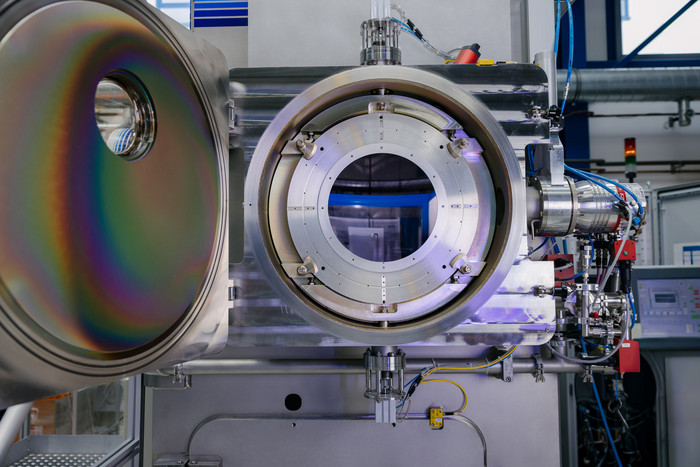
Ion Beam-assisted Patterning and Smoothing
Precise material removal down to the sub-nanometer range — essential for semiconductor manufacturing.
Laser-assisted Micro- and Nanostructuring
Laser-based micro- and nanostructuring for photonics and functional surfaces.
Free-form optics for high-performance systems
Nanometer-precision shaping for lithography, lasers, and space optics
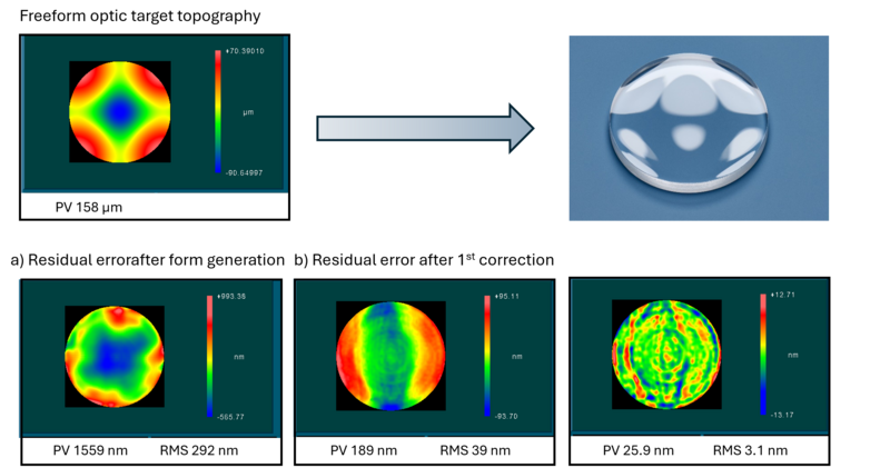
The fabrication of high-precision optical surfaces with complex geometries—particularly free-form surfaces—represents a key challenge for modern optical systems. Applications range from EUV lithography to high-power lasers and space telescopes.
At the IOM, beam-based processes such as ion beam milling and plasma jet etching are used for this purpose, enabling non-contact and locally highly precise surface correction. These methods allow for targeted optimization across all relevant scales—from global shape to nanoscale roughness.
A current focus is on researching the combination of physical and chemical etching mechanisms, for example through the use of reactive gases or hybrid processes. This can induce new interaction effects to significantly expand the range of processable materials or increase processing speed.
Result:
- Shape accuracy down to the sub-nanometer range
- Significantly improved optical performance
- Transferability to industrial manufacturing processes
Plasma jet processing for fast and scalable processes
Ultra-precision without a vacuum—efficient and industry-ready
Vacuum-based processes offer the highest precision but are often time-consuming and costly. That is why the IOM is developing alternative approaches such as plasma jet machining at atmospheric pressure.
This technology enables significantly higher removal rates—in some cases by several orders of magnitude—while simultaneously reducing the complexity of the equipment. Through targeted process control, even challenging materials can be machined with precision.
The processes are continuously being refined to optimize both surface quality and process stability and to make them suitable for industrial applications.
Result:
- Process speeds up to 100–1,000 times faster compared to ion beam processes
- Reduced system complexity
- High potential for industrial scaling
Ultra-smooth surfaces achieved through ion beam planarization
Targeted reduction of nanometer-scale roughness for maximum optical quality
For many optical applications, extremely low surface roughness is crucial for minimizing scattering losses and maximizing performance.
At the IOM, various approaches are being pursued for this purpose: (a) smoothing through direct ion bombardment, which utilizes various surface relaxation processes—particularly in the high-frequency spatial frequency range—and (b) the combination of sacrificial layers and ion beam processing for the targeted planarization of structured surfaces.
In the latter process, specially developed planarization layers are deposited and then selectively removed, so that the surface structure is smoothed and can be precisely transferred to the substrate
Result:
- Reduction of high-frequency roughness components to < 0.1 nm RMS through direct smoothing
- Ion beam planarization for larger spatial wavelengths to < 0.5 nm RMS
- Stable and reproducible processes even for complex structures

Micro- and nanostructuring via ion-beam-assisted pattern transfer
High-precision structured surfaces are of enormous importance for many optical applications. The key technology here is reactive ion beam etching (RIBE), which enables significantly more flexible process steps compared to purely inert ion beam etching (IBE). Customized RIBE process steps are being developed that allow for a wide range of profile shapes, particularly for diffraction gratings or pulse compression gratings.
Result:
- Ultra-flat surface profiles with structural amplitudes < 10 nm and blaze angles < 1° for etching processes with very low selectivities
- Etching of deep structures at high selectivities
- Highly homogeneous processing of optical components with ±1% depth accuracy (currently on 450 mm × 450 mm areas, with a future target of 1000 mm × 1000 mm)
Laser-based precision machining of optical components
Innovative laser plasmas for photonic manufacturing
The increasing demands on optical and photonic surfaces require the continuous development of novel processing methods. In addition to the sheer intensity of the tool effect, the key challenges for future processes include, above all, precise controllability and non-contact tool interaction.
At the IOM, laser-induced plasmas are being researched as an innovative processing tool for this purpose. The extremely high intensities of modern ultrashort-pulse lasers make it possible to precisely ignite free-standing microplasmas in gas atmospheres without electrical discharges.
The plasma serves as a high-precision etching agent for material removal at the atomic level. Because the size of the plasmas ranges from 10 to 100 µm, it is possible to machine structures that are difficult to address using conventional methods.
Result:
- Highest precision: Excellent process control due to a minimal average ablation rate in the range of a few picometers per laser pulse (pm/pulse)
- High surface quality: Ultra-smooth surface morphology with roughness values below 2 nm RMS and no structural defects
- High scalability: Efficient area processing through the use of high-repetition-rate laser sources