Tailored surfaces

Key technology for lithography through high-precision surface processing
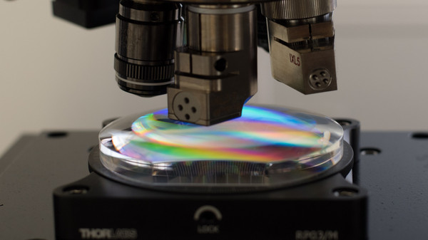
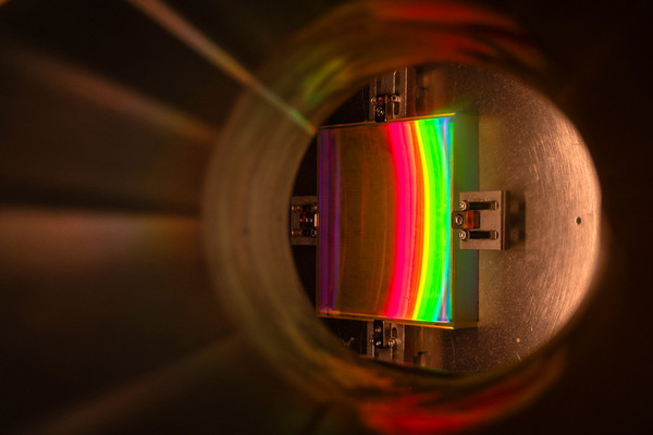
Ion beam technologies are a central foundation for the manufacture of high-precision optical components — particularly for applications in semiconductor lithography, photonics, and microelectronics. They enable the processing of surfaces with accuracies down to the sub-nanometer range and thus make a direct contribution to the next generation of high-performance microchips.
Physical fundamentals and process development
- Development and optimization of ion beam-based etching and removal processes
- Investigation of reactive and inert ion beam processes from a physical perspective
- Smoothing, patterning, and targeted material removal at the atomic scale
- Further development of broad-beam ion sources and simulation-based processes
Key technology for lithography and photonics
- Optics for lithography and modern semiconductor manufacturing
- High-precision components for photonics and laser applications
- Functional surfaces for demanding industrial applications
Precision, variety of materials, and scalability
- Precision down to less than one nanometer
- Wide range of materials:
Glasses, glass-ceramics, oxides, semiconductors, metals, polymers, and layered systems - Close integration of fundamental understanding and technological implementation
- Scaling of processes from the laboratory scale to large areas
Projects
10ÅCe - 10 Ångstrom CMOS exploration
microelectronics is a key technology for digitalization and crucial to Europe’s technological sovereignty. As part of the “European Partnership for Microelectronics Research and Technology,” the EU funds research projects such as the “10 Ångstrom CMOS exploration” project. In Germany, the focus is on multifunctional electronic systems, energy-efficient power electronics, and complex design. The IOM contributes to the improvement of EUV mirrors using ion-beam-based etching technologies, thereby strengthening the innovative capacity and competitiveness of the research institution as well as industry in Saxony.
Funded by the EU project 10ÅCe, the Chips Joint Undertaking and its members—the BMFTR, the SMWA, the Netherlands, Belgium, Germany, France, Austria, Ireland, and Israel
AD-ION - Advances in ion-surface interaction-driven manufacturing of one-dimensional metal oxide heterostructures
This collaborative project investigates a new approach to additive 3D manufacturing of complex nanoscale materials using ion-assisted deposition. An assist ion source is used in three stages: (1) for pre-structuring via ion beam erosion, (2) for phase and stoichiometry control via ion-assisted reactive processes, and (3) for final finishing of the geometry via ion beam polishing. The focus is on ZrO2-MoO3-X heterostructures, which are important for sensor technology, photonics, and quantum applications.
Funded by the NSF (U.S. National Science Foundation) and DFG
Monolithic binary and blaze lattices on silicon and oxides (MOBBS)
The overall goal of the project is to establish novel ion-beam-based fabrication methods that can be used to create inclined surface profiles for diffractive optical elements that are not achievable with current technologies. In line with potential related applications, two research areas are being systematically investigated: (1) the development and establishment of two novel, mutually complementary patterning methods for monolithic silicon blazed gratings, and (2) the development of an additional specialized oblique etching process.
Funded by BMFTR as part of the “WIR! – Change Through Innovation in the Region” funding program
nanoAR - Anti-reflective metasurfaces on materials with a large bandgap
In this research project, nine partners from industry and academia are developing methods to improve optical components. The collaborative project is funded as part of the “Basic Technologies for Fusion—Toward a Fusion Power Plant” funding program.
To pave the way for viable solutions, the project partners are, on the one hand, focusing on nanostructured or nanoporous anti-reflective coatings based on materials with a high bandgap, which are intended to ensure the necessary resistance to laser radiation. On the other hand, they are testing a subtractive approach: Instead of combining a substrate material with multiple anti-reflective layers applied to it, they are using lenses made of a single material that is intended to achieve the desired anti-reflective properties through appropriate nanostructuring of its surface. Using two wide-bandgap materials (quartz glass and calcium fluoride) as examples, corresponding large-area demonstrators for various wavelengths and pulse durations are to be developed. Their approaches could also be applied to other areas of application for high-performance optics.
Gefördert durch BMFTR
RISQ-DIAP - Diagnostics Platform
RISQ-DIAP is the IOM Leipzig diagnostic platform for reactiveion beametching (RIBE). It enables the comprehensive characterization and process-oriented optimization of broad-beam ion sources and RIBE processes—including the targeted adjustment of beam composition, energy, and angular distributions, as well as the evaluation of process stability and reproducibility. RISQ-DIAP thus lays the foundation for ultra-precise ablation, patterning, and smoothing processes with high dimensional accuracy and low surface roughness, and supports the development of application-specific processes for sophisticated optical components and other high-tech applications.
Funded by EFRE/SAB

O-ISA Reactive Ion Beam Etching System
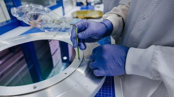
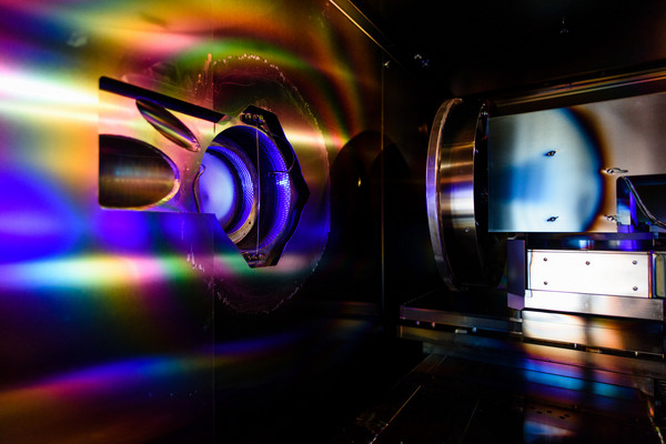
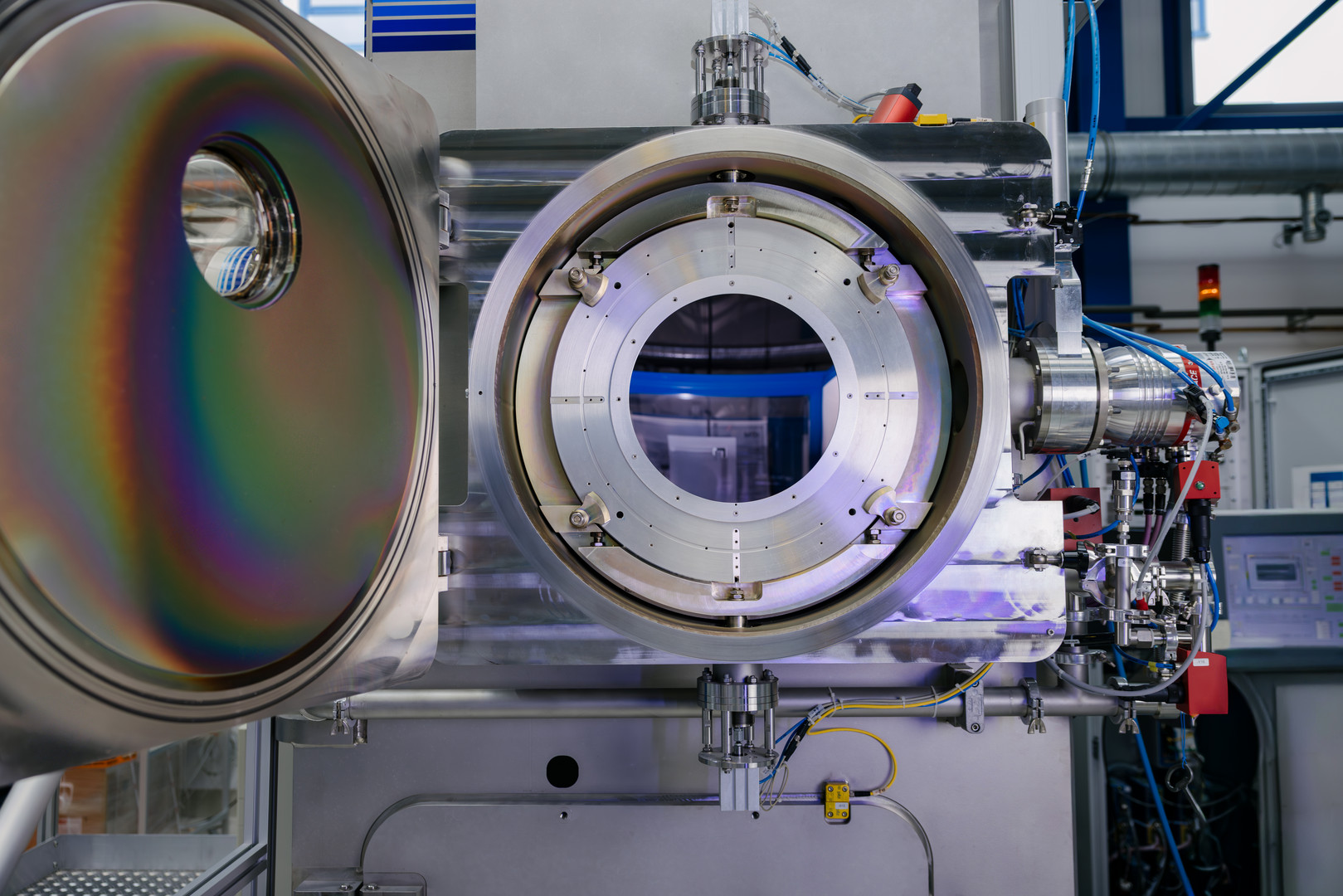
As part of the ERDF – Europe Supports Saxony, the Free State of Saxony (Sächsische Aufbaubank – SAB) is investing funds from the European Regional Development Fund (ERDF) in the expansion and improvement of the research infrastructure at the IOM, thereby ensuring the further strengthening of the IOM’s innovative capacity and enhancing its national and international visibility. The new facility will be used to address both application-oriented and fundamental research questions related to reactive ion beam etching (RIBE)—particularly on optical components with diameters of up to 200 mm. In doing so, the IOM is laying the groundwork for implementing ultra-precise machining processes with depth accuracies in the angstrom range at a new level of quality. A particular focus is on the development of processing methods for laser optics intended for high-power applications, such as the anti-reflection coating of optics and the fabrication of pulse compression gratings. These components are essential for future key technologies, such as the development of future laser inertial fusion power plants.
Funded by EFRE/SAB
TRADES - Training & Research in Advanced Dispersion Engineered grating-waveguide Structures
This doctoral training network, comprising eight European partners, addresses the current shortage of skilled professionals in the field of photonics through a structured research and training program for doctoral students. In the program, 15 doctoral students are developing innovative optical components based on waveguide structures with sub-wavelength gratings for high-power laser applications. State-of-the-art deposition, lithography, and etching techniques are used to optimize manufacturability, efficiency (> 99.9%), and laser damage threshold (> 1 J/cm²) for sub-picosecond pulses. At the IOM in particular, ion beam methods for fabricating diffractive structures are being investigated. In addition, the fellows receive practical training in innovation management, entrepreneurship, and commercialization to prepare them for careers in photonics research and development.
Funded by the EU and Mediation Centre Stakeholder Network (MCSN)

10ÅCe - 10 Ångstrom CMOS exploration
microelectronics is a key technology for digitalization and crucial to Europe’s technological sovereignty. As part of the “European Partnership for Microelectronics Research and Technology,” the EU funds research projects such as the “10 Ångstrom CMOS exploration” project. In Germany, the focus is on multifunctional electronic systems, energy-efficient power electronics, and complex design. The IOM contributes to the improvement of EUV mirrors using ion-beam-based etching technologies, thereby strengthening the innovative capacity and competitiveness of the research institution as well as industry in Saxony.
Funded by the EU project 10ÅCe, the Chips Joint Undertaking and its members—the BMFTR, the SMWA, the Netherlands, Belgium, Germany, France, Austria, Ireland, and Israel
Publication highlights
G. Dornberg, E. Rohkamm, P. Birtel, F. Scholze, F. Frost
Characterization of a broad beam Kaufman-type ion source operated with CHF3 and O2
J. Vac. Sci. Technol. A 41 (2023) 053104, DOI: 10.1116/6.0002766
Process stability is crucial for precise reactive ion beam etching in optics. A Kaufman ion source using CHF₃/O₂ was characterized and its performance correlated with etching results on SiO₂, Si, and photoresist. Etching selectivity depends heavily on the composition of the ion beam, which varies with the beam current and gas flow rate even at constant gas mixture ratios.
F. Linß, C. Bundesmann, F. Frost
Low-energy ion beam erosion of Si with simultaneous co-deposition of metallic surfactants: Experimental and simulated data
Appl. Surf. Sci. 646 (2024) 158923, DOI: 10.1016/j.apsusc.2023.158923
Ion beam erosion of Si with simultaneous co-deposition results in surface patterns at the nano- and micro-scales. Using low-energy Ar ions and various metals, SEM and AFM measurements show that silicide-forming metals induce patterning and higher roughness, while others do not. The Si ablation rates depend on the atomization and scattering properties of the co-deposited material.
E. Rohkamm, D. Spemann, F. Scholze, F. Frost
Influence of the RF-power on the etching yields and surface morphology in reactive ion beam etching of Si and photoresist
J. Appl. Phys. 136 (2024) 193302, DOI:10.1063/5.0233226
The ion energy distribution and composition of an HF-excited ion beam using CHF₃/O₂ were investigated and correlated with the etching behavior. Energy-resolved mass spectrometry, current density, and etch rate measurements were performed on Si and photoresist. Higher HF power increases the plasma density, enhances gas fragmentation, alters the surface chemistry, and significantly affects the etch yield and photoresist morphology.
L.P. Lingenfelder, A. Finzel, G. Dornberg, J. Zajadacz, F. Frost
Enhanced planarization technology by reactive ion beam etching and using a nanoimprint resist
Appl. Phys. A 131 (2025) 463, DOI: 10.1007/s00339-025-08540-9
Ultra-smooth optical surfaces are essential for high-quality optics. This study investigates ion beam planarization using a low-viscosity nanoimprint resist to remove rotational traces from SPDT-fabricated surfaces. Compared to standard photoresist, the nanoimprint resist exhibits superior leveling across all spatial wavelengths and enables successful etch transfer, reducing the RMS roughness from 13 nm to 0.5 nm.
P. Birtel, E. Rohkamm, J. Bauer, F. Frost
Influence of water background pressure on removal rates of SiO2, Si and photo resist in reactive ion beam etching
Surf. Interfaces 64 (2025) 106306, DOI: 10.1016/j.surfin.2025.106306
Process stability in reactive ion beam etching is of critical importance for optical manufacturing. This study investigates the influence of residual water on the etching of SiO₂, Si, and photoresist using CHF₃/O₂. Water alters the composition of the ion beam and the formation of the near-surface layer, which affects etch yield and selectivity. These systematic changes have important technological implications for process control.
Equipment
- Optik-ISA: RIBE system for substrates up to 125 mm in diameter, Kaufman ion source
- ISA-III: RIBE system for substrates up to 100 mm in diameter, Kaufman ion source
- ISA200: RIBE system for substrates up to 200 mm in diameter, Kaufman ion source
- SHAPION: RIBE system for substrates up to 200 mm in diameter, Kaufman ion source
- RIBE-450: RIBE system for substrates up to 450 mm in diameter, Kaufman ion source
- EUVL: RIBE system for substrates up to 300 mm in diameter, RF ion source
- RISQ-DIAP: Diagnostic platform for RIBE processes, substrates up to 500 mm, RF ion source
- O-ISA 200: RIBE system for substrates up to 200 mm in diameter, RF ion source (available starting 12/2026)
- RIBF1000: RIBE system for substrates up to 1000 mm in size, various RF ion sources (available starting 12/2026)
- ICON PT AFM
- ICON/Fastscan AFM
- DME AFM System
- Reflectometer
- White-light interferometer NPFlex
- Mechanical Profiler XT
Videos
Click on the image to play the video. The video plays via YouTube.